
6.1 Design problem
Work your assigned combinational logic design problem using the DirectVHDL simulator and the following procedure:
- Work out the logic design for your assigned problem, including a block diagram for the main module showing inputs, outputs, and internal connections.
- Write VHDL code that describes your design.
- Simulate and debug the VHDL code.
- Print out a simulator listing that verifies the correct operation of your design for the prescribed test sequences.
Design Problem 1
A half adder is a circuit that can add two bits at a time to produce a sum and a carry. Design a half adder using only two gates. Write an entity-architecture pair to implement the half adder. Now write an entity-architecture pair to implement a full adder using two instances of your half adder and an OR gate. Use the port definitions specified below:
For the half adder: port (a, b: in bit; s, c: out bit);
For the full adder: port (a, b, cin: in bit; sum, cout: out bit);
Simulate your code and test it using the following inputs: a b cin = 001, 011, 111, 110, 100
Design Problem 2
a. The diagram shows an 8-bit shifter that shifts its input one place to the left. Write a VHDL module for the shifter.
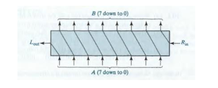
b. Write a VHDL module that multiples an 8-bit input (C) by 1012 to give an 11-bit product (D). This can be accomplished by shifting C two places to the left and adding the result to C. Use two of the modules written in (a) as components and an overloaded operator for addition.
c. Simulate your code and test it using the following inputs: 10100101 11111111
Design Problem 3
a. Write a VHDL module for a 4-bit adder, with a carry-in and carry-out, using an overloaded addition operator and std_logic_vector inputs and outputs.
b. Design an 8-bit subtracter with a borrow-out, using two of the 4-bit adders you designed in (a), along with any necessary gates or inverters. Write a VHDL module for the subtracter.
c. Simulate your code and test it using the following inputs: 11011011-01110110, 01110110-11011011
6.2 Design problem 2
In the previous module, you were asked to design and simulate a combinational circuit using NAND and NOR gates. In this assignment, we ask you to convert your SimUaid circuit from the previous module to VHDL code, compile the VHDL code, download it to the Basys 3 FPGA board, and test its operation.
One of the features of SimUaid is the automatic conversion of circuit diagrams to VHDL. The VHDL converter removes all switches, probes, and other I/O devices from the circuit, and puts the corresponding signals into the input and output ports of a VHDL module. Each SimUaid component is instantiated as a VHDL component and the signals that connect to the component inputs and outputs are placed in the component port. The resulting VHDL code can be compiled and synthesized using the appropriate software. The necessary VHDL components are defined in the SimUaid synthesis libraries that are installed in the lib folder of your DirectVHDL installation. We use the Vivado software to synthesize the VHDL code and download it to the Basys 3 FPGA board.
Each student should perform this activity.
Once you have completed this activity, select the assignment link and use the assignment text box to verify that you have completed the code download of your FPGA board.