
5.2 Design Problem:
Your instructor will assign you to work one of the four design problems and also assign you a lab partner. If there are an odd number of students, there may be one group with three students partnering. Use the Module 5 Discussion Board for all lab-related collaboration with your lab partner(s). Please provide only one submission for both of you and your lab partner(s). Provide details on the work done by each student.
Work your assigned combinational logic design problem using the following procedure:
- Derive a truth table for the assigned problem.
- Use Karnaugh maps to derive logic equations in sum-of-products or product-of-sums form depending on whether NAND gates or NOR gates are required.
- Enter the truth table into LogicAid, derive the logic equations, and check the answers against the results of step (2).
- Draw a circuit of AND and OR gates, trying to minimize the number of gates required by using common gates as appropriate. Factoring or multiplying out is required in some cases.
- Convert to NAND or NOR gates as specified.
- Simulate your answer to (5) using SimUaid, and verify that the circuit works correctly. Use switches as inputs and probes or a 7-segment indicator as outputs.
Submit a SimUaid circuit that meets the problem specifications, the truth table and equations derived using LogicAid, and the Karnaugh maps.
Design Problem 1
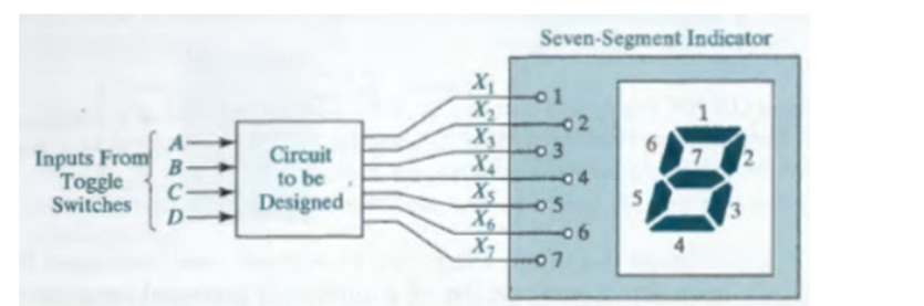
Design an 8-4-2-1 BCD code converter to drive a seven-segment indicator. The four inputs to the converter circuit (A, B, C, and D in the figure above) represent an 8-4-2-1 binary-coded-decimal digit. Assume that only input combinations representing the digits 0 through 9 can occur as inputs so that the combinations 1010 through 1111 are don’t-cares. Design your circuit using only two-, three-, and four-input NAND gates and inverters. Try to minimize the number of gates required. The variables A, B, C, and D will be available from toggle switches.
Design Problem 2
Work Design Problem 1, except use 4-2-1-8 code instead of 8-4-2-1 code. For example, in 4-2-1-8 code, 9 is represented by 0011. Also, change the representations of digits 6 and 9 to the opposite form given in Problem 1. Any solution with 20 or fewer gates and inverters (not counting the four inverters for the inputs) is acceptable.
Design Problem 3
Work Design Problem 1 using two-, three-, and four-input NOR gates and inverters instead of NAND gates and inverters. Any solution that uses 19 gates and inverters or fewer (not counting the four inverters for the inputs) is acceptable.
Design Problem 4
Work Design Problem 2 using two-, three-, and four-input NOR gates and inverters instead of NAND gates and inverters. Any solution that uses 17 gates and inverters or fewer (not counting the four inverters for the inputs) is acceptable.